

Measurement Utility
innovative, all-in-one measurement solution.
Measurements
Yes, we can measure practically everething!
-
Measurement Algorithms:
Gray Level, Gradient
-
Image preprocessing:
Linear, Adaptive, Kernels
-
Waveform Fit:
Gaussian, Wavelet, NN coders (patented).
-
Denoising:
Classical with self convergence of parameters.
Blind denoiser with Self supervision (patented).
-
Features to measure:
Line/Space/Contact/Pillar/Free Hand/Rotated
/PSD/Overlay/Resolution/SNR/


Denoising AI
Deep structures by Blind Decomposition:
An exceptional solution for detecting weak signals in the bottom region of deep structires.
Capable of measuring the slant of deep cuts/trenches or the bottoms of contacts, even in highly challenging cases involving extremely deep SEM images. Expected detection limit at 3% of full dynamic span of the image.
Measuring Resolution and SNR
Resolution Measurement:
Measurement Utility in not only measuring image resolution more robustly than the vendor-supplied "in tool" applications but also extending it to resolution measurements of CD (Critical Dimension) targets.
By using a Measurement utility that is not reliant on vendor-specific applications, you can achieve a more robust and independent assessment of resolution. This allows for greater confidence in the accuracy and reliability of the measured values.. While vendors may provide "in tool" applications for resolution measurement, having an independent measurement utility offers several advantages. Being able to measure resolution and CD targets within a single measurement enhances efficiency and provides a comprehensive understanding of the manufacturing process. Additionally, we can predict CD readings for any required "beam shape" values.


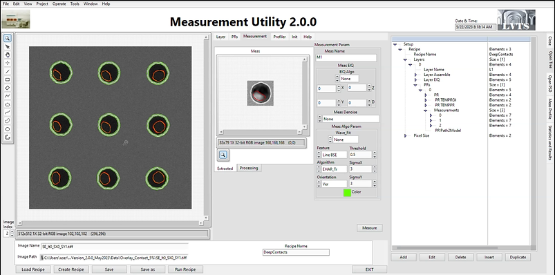
Creating recipes made incredibly easy
Measurement Utility build around advanced CDSEM measurement flow based on Pattern recognition and Measurement vector transfer. The difference that all OEM manufacturers offer 1Layer-1PR-NMeas approach. We are offering NLayers-NPRs-NMeas scheme - means that you have multiple ways for recipe creation and gradual imporvements. Measurement Utility could be programmed to perform almost any required CDSEM measurement just by creating simple recipe by local technicians after 3 days of training.
Mass Measurement
We can do mass measurement.
Mass measurement can indeed be performed for various purposes in semiconductor manufacturing, including stochastic definition and defects inspection.
Stochastic definition refers to the statistical analysis of variations in mass distribution within a semiconductor wafer.Mass measurement can provide valuable information about process variations and potential sources of defects. By analyzing the mass distribution, manufacturers can gain insights into the uniformity and consistency of the manufacturing process, leading to process improvements and enhanced yield.
Defects inspection is another important application of mass measurement. By measuring the mass of individual features or structures on a semiconductor wafer, manufacturers can identify and classify defects. Deviations in mass can indicate the presence of contaminants, irregularities, or other defects that can affect the performance or reliability of the fabricated devices.


EPE Support
Measuring non-common CD (Critical Dimension) metrology structures, such as high elongated contacts, angles, curvatures, corners, hemispheres, etc., can indeed provide added value in controlling EPE (Edge Placement Error) during semiconductor manufacturing.
EPE refers to the deviation of patterned features from their intended positions on a semiconductor wafer. It is a critical parameter that affects the performance and functionality of integrated circuits. By accurately measuring the CDs of various non-common structures, manufacturers can gain better control over EPE, leading to improved device performance, yield, and overall manufacturing quality.
Deep Structures
Measuring slant and overlay in deep trenches and contacts is indeed an important aspect of semiconductor manufacturing. Slant refers to the angular deviation of the trench or contact sidewalls from the vertical direction, while overlay refers to the alignment accuracy between different layers or patterns on a semiconductor wafer.
We include newly designed Blind Denoising by Self Supervision to deal with that issue.
By employing these AI filters, N-2/N-3 tool generations can be made capable of supporting new processes and measurements. This means that even older tools, which may not have been originally designed to handle the specific requirements of newer processes, can be upgraded to support them. This can provide a significant leverage in manufacturing procedures, as it allows for the utilization of existing tools without the need for complete replacement or expensive upgrades.

True PSD Measurement
PSD Measurement:
The implementation of a unique denoising AI module for achieving True PSD (Power Spectral Density) measurement offers an alternative approach to traditional methods, including those used by Fractilia.
Power Spectral Density is a measure of the distribution of power in a signal as a function of frequency. Accurate measurement of PSD is crucial in various fields, including semiconductor manufacturing, where it helps assess the quality and performance of fabricated devices.
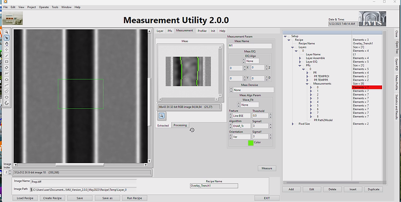
Overlay Measurement
We can measure SEM overlay:
The new method, designed for precise and accurate Backscattered Electron (BSE) and Secondary Electron (SE) image overlay calculation, provides an innovative approach to overlay measurement. BSE and SE images are commonly captured in SEM imaging and can provide valuable information about the topography and features of a sample.
By utilizing these SEM images, our method offers a simpler way to measure overlay, potentially streamlining the measurement process and reducing complexity compared to traditional methods. The simplicity of the method can lead to improved efficiency and productivity in semiconductor manufacturing processes.


Why LVTailoring?
Same Hardware
No need for new, highly-specialized, and expensive hardware
Same System
Re-invest in the power of your business with our innovative solution
New Capabilities
Control your capital costs, solve your performance issues and achieve your goals with ease
Save your capital dollars.
Allow us to unlock the full potential of your existing tools – using the same system, same hardware , and new software - for brand new capabilities.